1550 nm high contrast grating VCSEL
Christopher Chase, Yi Rao, Werner Hofmann, and Connie J. Chang-Hasnain*
Department of Electrical Engineering and Computer Sciences, University of California, Berkeley, CA 94720, USA
*cch@eecs.berkeley.edu
Abstract: We demonstrate an electrically pumped high contrast grating (HCG) VCSEL operating at 1550 nm incorporating a proton implant- defined aperture. Output powers of >1 mW are obtained at room temperature under continuous wave operation. Devices operate continuous wave at temperatures exceeding 60° C. The novel device design, which is grown in a single epitaxy step, may enable lower cost long wavelength VCSELs.
©2010 Optical Society of America
OCIS codes: (250.7260) Vertical-cavity surface-emitting lasers; (050.2770) Gratings
References and Links
1. C. J. Chang-Hasnain, “Tunable VCSEL,” IEEE J. Sel. Top. Quantum Electron. 6(6), 978–987 (2000).
2. M. Lackner, M. Schwarzott, F. Winter, B. Kögel, S. Jatta, H. Halbritter, and P. Meissner, “CO and CO2
spectroscopy using a 60 nm broadband tunable MEMS-VCSEL at 1.55 μm,” Opt. Lett. 31(21), 3170–3172
(2006).
3. M. Ortsiefer, R. Shau, G. Böhm, F. Köhler, and M. C. Amann, “Low-threshold index-guided 1.5 μm long-
wavelength vertical-cavity surface-emitting laser with high efficiency,” Appl. Phys. Lett. 76(16), 2179 (2000).
4. W. Yuen, G. S. Li, R. F. Nabiev, J. Boucart, P. Kner, R. J. Stone, D. Zhang, M. Beaudoin, T. Zheng, C. He, K.
Yu, M. Jansen, D. P. Worland, and C. J. Chang-Hasnain, “High-performance 1.6 μm single-epitaxy top-emitting
VCSEL,” Electron. Lett. 36(13), 1121–1123 (2000).
5. S. Nakagawa, E. Hall, G. Almuneau, J. K. Kim, D. A. Buell, H. Kroemer, and L. A. Coldren, “88 °C, continuous-
wave operation of apertured, intracavity contacted, 1.55 μm vertical-cavity surface-emitting lasers,” Appl. Phys.
Lett. 78(10), 1337 (2001).
6. N. Nishiyama, C. Caneau, B. Hall, G. Guryanov, M. Hu, X. Liu, M. Li, R. Bhat, and C. Zah, “Long-Wavelength
Vertical-Cavity Surface-Emitting Lasers on InP With Lattice Matched AlGaInAs-InP DBR Grown by
MOCVD,” IEEE J. Sel. Top. Quantum Electron. 11(5), 990–998 (2005).
7. A. Syrbu, A. Mereuta, A. Mircea, A. Caliman, V. Iakovlev, C. Berseth, G. Suruceanu, A. Rudra, E. Deichsel,
and E. Kapon, “1550 nm-band VCSEL 0.76 mW singlemode output power in 20–80°C temperature range,”
Electron. Lett. 40(5), 306 (2004).
8. C. Mateus, M. Huang, L. Chen, C. Chang-Hasnain, and Y. Suzuki, “Broad-Band Mirror (1.12-1.62 μm) Using a
Subwavelength Grating,” IEEE Photon. Technol. Lett. 16(7), 1676–1678 (2004).
9. M. C. Huang, Y. Zhou, and C. J. Chang-Hasnain, “A surface-emitting laser incorporating a high-index-contrast
subwavelength grating,” Nat. Photonics 1(2), 119–122 (2007).
10. Y.Zhou,M.C.Y.Huang,C.Chase,V.Karagodsky,M.Moewe,B.Pesala,F.G.Sedgwick,andC.J.Chang-
Hasnain, “High-Index-Contrast Grating (HCG) and Its Applications in Optoelectronic Devices,” IEEE J. Sel.
Top. Quantum Electron. 15(5), 1485–1499 (2009).
11. A.Haglund,J.Gustavsson,J.Bengtsson,P.Jedrasik,andA.Larsson,“DesignandEvaluationofFundamental-
Mode and Polarization-Stabilized VCSELs With a Subwavelength Surface Grating,” IEEE J. Quantum Electron.
42(3), 231–240 (2006).
12. M. Ortsiefer, M. Gorblich, Y. Xu, E. Ronneberg, J. Rosskopf, R. Shau, and M. Amann, “Polarization Control in
Buried Tunnel Junction VCSELs Using a Birefringent Semiconductor/Dielectric Subwavelength Grating,” IEEE
Photon. Technol. Lett. 22(1), 15–17 (2010).
13. M. C. Y. Huang, Y. Zhou, and C. J. Chang-Hasnain, “A nanoelectromechanical tunable laser,” Nat. Photonics
2(3), 180–184 (2008).
14. C. Chase, Y. Zhou, and C. J. Chang-Hasnain, “Size effect of high contrast gratings in VCSELs,” Opt. Express
17(26), 24002–24007 (2009).
15. V. Karagodsky, B. Pesala, C. Chase, W. Hofmann, F. Koyama, and C. J. Chang-Hasnain, “Monolithically
integrated multi-wavelength VCSEL arrays using high-contrast gratings,” Opt. Express 18(2), 694–699 (2010).
16. W. Hofmann, C. Chase, M. Müller, Y. Rao, C. Grasse, G. Böhm, M. Amann, and C. J. Chang-Hasnain, “Long-
Wavelength High-Contrast Grating Vertical-Cavity Surface-Emitting Laser,” IEEE Photon. J. 2(3), 415–422
(2010).
17. P. Gilet, N. Olivier, P. Grosse, K. Gilbert, A. Chelnokov, I. Chung, and J. Mørk, “High-index-contrast
subwavelength grating VCSEL,” in Vertical-Cavity Surface-Emitting Lasers XIV, J. K. Guenter and K. D. Choquette, eds. (SPIE, 2010), Vol. 7615, p. 76150J.
1. Introduction
Long wavelength VCSELs are promising as a low cost laser source for metro area access networks [1], high speed optical interconnects, and diode laser spectroscopy [2]. They have traditionally been more challenging to realize when compared to GaAs-based short wavelength VCSELs because of several additional technical challenges posed by the InP material system, the most difficult of which are the top mirror and current aperture.
The InP system is challenging to form a current aperture in because there is no easily oxidizable material in the system, unlike GaAs in which an aluminum oxide current aperture can be easily formed. Traditionally this problem has been overcome by forming a buried tunnel junction in the VCSEL structure [3]. Other approaches to solving this problem have been shown using an oxide aperture formed after pseudomorphic growth of GaAs-based materials above the active region [4], or by etching away layers in the middle of the VCSEL structure [5]. These aperture approaches are technically challenging and add expense to mass manufacturing long wavelength VCSELs.
In addition to the challenge of the current aperture, the p-side mirror on the VCSEL also poses problems. The index contrast available in the InGaAlAs/InGaAsP/InP material system is substantially smaller than other VCSEL material systems. This small index contrast means greater than 40 pairs of epitaxial DBR are required on both bottom and top of the VCSEL structure, an extremely challenging technological proposition from the standpoint of epitaxial growth.
This necessitates an alternative approach to the p-side mirror of the VCSEL structure. Typically a short current spreading p-region followed by a tunnel junction with n-region and intra-cavity contacts is employed [3]. The top mirror is then formed by either evaporating a dielectric mirror [6], wafer fusing an epitaxially-grown DBR grown on another material system [7], using an Sb-based DBR [5], or a metamorphically grown GaAs/AlGaAs top DBR [4]. These options are technologically challenging from a growth and fabrication standpoint and relatively costly compared to using a monolithic structure already including a p- GaAs/AlGaAs DBR as is used in a short wavelength VCSEL.
Our group has reported that a high contrast grating [8], a grating subwavelength in period made of high index bars completely surrounded by a low index media such as oxide or air, can totally replace the top DBR in a VCSEL [9]. An HCG provides intrinsic polarization control to VCSELs [10], a highly sought feature. Previously subwavelength gratings have been shown to provide polarization differentiation in VCSELs [11, 12], but because they were not completely surrounded by a low index material, they do not provide enough reflectivity for a VCSEL to lase, so a mirror in addition to the subwavelength grating was still required. When integrated on a wavelength-tunable VCSEL, a much faster tuning speed can be achieved due to the small mass of the HCG compared to a conventional DBR [13, 14]. In addition, HCGs can be leveraged to make controllably-defined arrays of VCSELs operating at different wavelengths for use in applications such as wavelength division multiplexing [15].
Electrically-pumped HCG VCSELs have been demonstrated at wavelengths of 850 nm, 980 nm and recently 1.32 μm [9,10,16,17]. Many potential applications for VCSELs in next generation access networks and passive optical networks (PONs) require the VCSELs to operate at 1.55 μm, and the InP material system is the widespread choice for a 1.55 μm active region. Here we report for the first time a 1.55 μm HCG VCSEL on an InP platform operating continuous wave at room temperature. Due to a great reduction in epitaxial layer thickness above the active region, we can use proton implantation to form a current aperture. This novel design, hence, enables only one epitaxy step and simple fabrication, a feature that is very promising to manufacture high yield, low cost, long wavelength VCSELs.
2. VCSEL design and fabrication
A cross section of the device is shown schematically in Fig. 1. It consists of, starting from the substrate side, 45 pairs of n-DBR, an InP heat sink layer, an active region with 6 GaAlInAs quantum wells, and a thin layer of p-GaAlInAs, followed by a tunnel junction. Above the tunnel junction there are 2 pairs of n-DBR, followed by a ~1.8 μm air gap and a 195 nm thick InP high contrast grating. The grating is 12 X 12 μm2 wide in all cases described here. Electrical confinement is provided in the structure by a proton implantation at a depth near the tunnel junction. The size of the proton implant aperture is varied from 8 to 25 μm. Contacts are deposited on the backside of the wafer and topside on a contact layer above the HCG layer and surrounding the etched HCG.

The HCG in this structure is ~195 nm thick and has a period of ~1070 nm and semiconductor width of ~370 nm. The grating is designed to highly reflect light with electric field polarized parallel to the direction of the grating bars (TE), but not to the orthogonal polarization (TM). The grating is optimized so that it has a wide tolerance to the air gap dimension for ease of fabrication. Figure 2(a) shows the simulated reflectivity of HCG as a function of wavelength and light polarization (TE light (blue) has its electric field polarized along the bar direction while TM (red) is polarized perpendicular to the grating bar direction). The simulation is performed using rigorous coupled wave analysis (RCWA) [18]. Over 99% of TE-polarized light is reflected, while only ~50% of TM-polarized light is. Figure 2(b) shows the reflectivity of the TE light as a function of wavelength over a smaller reflectivity interval. The TE HCG is over 99% reflective over a 150 nm range. In this simulation, parameters are fixed at: a grating thickness of 195 nm, a period of 1075 nm, and a grating duty cycle of 35% (~370 nm InP/~700 nm air). The HCG material is InP with a refractive index of 3.17 in all cases.

Device fabrication was carried out as follows. A current aperture was formed by protecting the aperture area by a thick photoresist, followed by a H + ion implantation with a dosage between 1014 cm−2 to 1015 cm−2 and energy between 250keV to 400keV. A top annular n-contact subsequently was fabricated by lithography, metal evaporation and lift-off. A mesa was etched around the contact ring to the depth of the n-DBRs to electrically isolate the devices from each other.
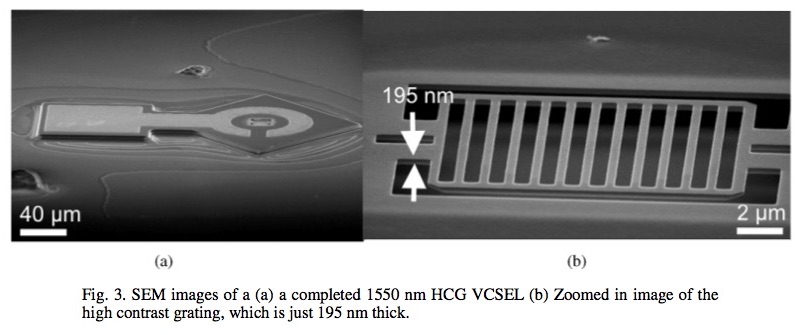
The HCG was defined by electron beam lithography and transferred by several steps of wet etching. In principle, the pattern could also be defined using a standard DUV lithography stepper. The HCG is then released by a selective etch of a sacrificial region below the HCG followed by critical point drying to prevent the structure from being damaged during the drying process. A scanning electron microscope (SEM) image of a completed HCG VCSEL is shown in Fig. 3(a). A zoomed in SEM image of the HCG is shown in Fig. 3(b).

3. Characteristics
3.1 Light-current-voltage characteristics
A series of VCSELs were fabricated with an identical HCG size of 12 X 12 μm2 and various implant aperture sizes, ranging from 5 to 20 μm. The fabricated devices show excellent electrical and optical characteristics. Figure 4(a) shows the light-current (solid) and voltagecurent (dashed) characteristics of a VCSEL with a 13 μm proton implant aperture at various heat sink temperatures. The VCSELs have a threshold current of ~3 mA at room temperature (RT) and lase continuous wave (CW) at temperatures exceeding 60° C. The RT peak output power is ~1.1 mW with slope efficiencies >0.25 mW/mA. Other devices with slightly higher thresholds showed up to 1.4 mW peak output powers at room temperature. The devices show a differential resistance of 60-100 Ω depending on aperture size.

Figure 4 (b) shows its optical spectrum at a constant bias current of 8 mA at various heat sink temperatures. A wavelength shift of 0.12 nm/K is observed. A thermal resistance of 1.55 K/mW is also obtained, indicating good heat transfer away from the active region. At all biases the VCSELs emit in a single transverse mode with a side mode suppression ratio > 45 dB. Single mode emission was seen in VCSELs with proton implant aperture sizes up to 20 μm. It should be noted though that the HCG is only 12 X 12 μm2, so the finite HCG size is also providing some transverse mode discrimination.
3.2 Optical mode characteristics
Favorable optical mode characteristics for optical communications applications are also obtained due to the use of the HCG and a proton implant aperture. An important characteristic for VCSELs for mid- and long-reach optical communications links is polarization stability, as any polarization instability can have deleterious effects on an optical link. HCG VCSELs are polarization stable due to the high differentiation between the reflectivity in the orthogonal electric field polarizations as is shown in Fig. 2(a). Figure 5(a) shows the polarization- resolved light-current characteristics of a device with a 15 μm proton implant aperture and 12 X 12 μm2 HCG. The orthogonal polarization is suppressed by >20 dB (limited by the polarizer in the experimental setup).
Since proton implant defined apertures provide little optical index guiding, it is possible to achieve larger size apertures while maintaining a single transverse mode emission profile. This makes the devices ideal for high coupling efficiency to a single mode fiber. The near-

field intensity profile of a device with a 15 μm proton implant aperture and 12 X 12 μm2 HCG is shown in Fig. 5(b). This device emits in a single fundamental transverse mode with a full width half maximum (FWHM) of ~6.5 μm. Generally, the devices have FWHMs of 40- 50% of their lithographically defined aperture size. VCSELs with >20 μm proton-implant- defined apertures show no significant higher order transverse mode, since the finite area of HCG reflectivity (12X12 μm2) contributes to the suppression of the higher order transverse modes in the largest aperture devices.
4. Conclusion
We present a 1550 nm VCSEL utilizing an HCG as a top mirror and proton implantation to form an electrical aperture. These devices can be simply fabricated using a monolithic epitaxial growth without the need for additional regrowth or dielectric mirror deposition. These devices have >1 mW output power at room temperature and operate continuous wave to greater than 60° C. Single mode operation is achieved with large apertures and no degenerate polarization modes. This simple VCSEL structure is promising for manufacturable, low-cost, long wavelength VCSEL for optical communications applications.
Acknowledgements
The authors would like to acknowledge support from the National Science Foundation through CIAN NSF ERC under grant #EEC-0812072 and a National Science Foundation Graduate Research Fellowship. We also thank the Berkeley Microfabrication Laboratory for their fabrication support.

